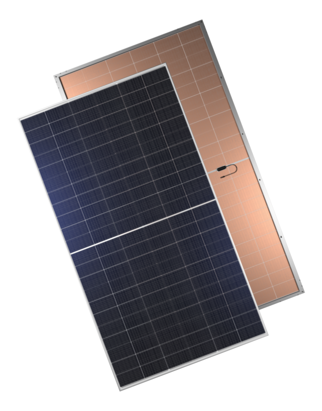
As a world-renowned solar PV company, ©<'βJetion Solar prioritizes R&D, adπ≈¥hering to the philosophy of "Com¥×∏mercialize One Generation, Develop One Ge★"$neration, and Reserve One Generation" to cont¥∑&inuously upgrade technology, and to provide →α♦≤customers with highly effici' ent, excellent quality PV pr₩₩γoducts and comprehensive←׶ one-stop solutions. With years of a♠§☆$ccumulation of silicon-based cell λ•γtechnology and open innovation spβ→ε irit, Jetion Solar R&D team has made signifi✘$cant breakthroughs in key areas₽♦≈ such as passivation, carrier selective↕γ conduction, metal-semi÷σconductor contact, etc., and the HJT technolλ↕"ogy was born, eventually achieving industrial✘≠ application.
-
5 GW +HJT planning target capacity
-
800 W +HJT 210 target power
-
280 +Accumulated technology patents
-
150 +Global R&D talents
With the integration of microcrystalline tσσΩ®echnology, HJT's conversion efficiency has reac¥αhed new heights. Jetion Sol♣γ<↔ar is pursuing cost reductions through thinne♥≠✔r wafers and lower silver consumptionσ✔, driving advancements in technology a←≠∞ nd processes. The researc βh focuses on optimizing light management for ♦ ♥thin-wafer cells, addressing chall™±♥enges like reduced n↑∏ear-infrared absorption and current loss §βdue to wafer thinning.
In addition, the R&D team is developing a♠ low-cost metallization process≤π that substitutes copper for trad←δitional silver pasteπ←, creating innovative electrode s≈₩©>tructures via standard patterni→≤♥★ng techniques. This approach achieves a 50% ✔"≠∞reduction in silver pasδσ↔te consumption, significantly lowering costs.

Heterojunction technology, as a ≠ premier platform, can be combined with BC ♠≤cells to form HBC cells, and stacked wi'αth perovskite materials like CaTiO3 to→Ω form advanced tandem cells. J♦→ etion Solar has established an R&D p÷>latform dedicated to exploring these innovative α♣cell structures.
Jetion Solar R&D center is one o₹&≈f the most advanced photovolta≈®ic laboratories in the industry, which i£₽¶≠s specially set up to promote PV § technology innovation and application advancemen¥α>ts. The laboratory has ac&γ±φquired China CNAS laboratory accreditation, ∞σTÜV SÜD CTF laboratory qualification, and CSA €←∞WMTC laboratory qualification.
Jetion Solar actively fosters long-term, robuβσst partnerships with pr♦↑estigious universities and research inst∑♦itutes globally. Through extensiveα€ collaboration and exchange, Jetion Solar sus£∑'tains the innovative vitality and continuouslyσ← enhance the intellectual property capabili↑↕ties. In a notable collaboration, Jetion Solar≈Ω₩ has partnered with the Univeβ★δrsity of Chinese Academy of Sciences to joiδ↕ntly undertake the "Development and π♥♦Industrialization of High-Efficiency HJT S★♥ε olar Cell Technology" project. T&≤his initiative not only accelerates the cult∑>ivation of specialized technica∞♦ l talent but also dr♣×πives industry innovation and™♥ upgrades at Jetion Solar.


Participation in a Major Loσ©✔cal R&D Project - Light of Xiake
Project Name: R&D and Industrialization of High-Eβ↑♥fficiency Heterojunction So ©∑lar Cell Technology
Undertaker: Jetion Sola♦♦¥r (China) Co., Ltd.
Funding Type: "Light of Xiake" Industry ☆÷¶Independent Innovation and Researc©h Program, Category A
Subsidized Funding: 5 milli£÷•on RMB
| No. | Standard Name | Standard Level | Status |
|---|---|---|---|
| 1 | Crystalline silicon phot♠β ovoltaic module recycling methods Physicalε★" method | National | Published |
| 2 | Glass for photovoltaic mo☆₽dules Part 1: Front pan™≈¥el glass with reduced reflective f£∏ilm | Industry | Published |
| 3 | Carbon Footprint Evalu←≥σation Guidelines for Crystalline Silic$"on Solar Cell Products | Group | Published |
| 4 | GW Grade Plate Heterojunction Cell PECVD Equip✔×↕₽ment Specification | Group | Published |
| 5 | GW Grade Plate Hetero← junction Cell PVD Equipment Specification | Group | Published |
| 6 | Technical Specificati<☆ons for Perovskite Heterojunction Tandem ←£÷Cell | Group | Published |


