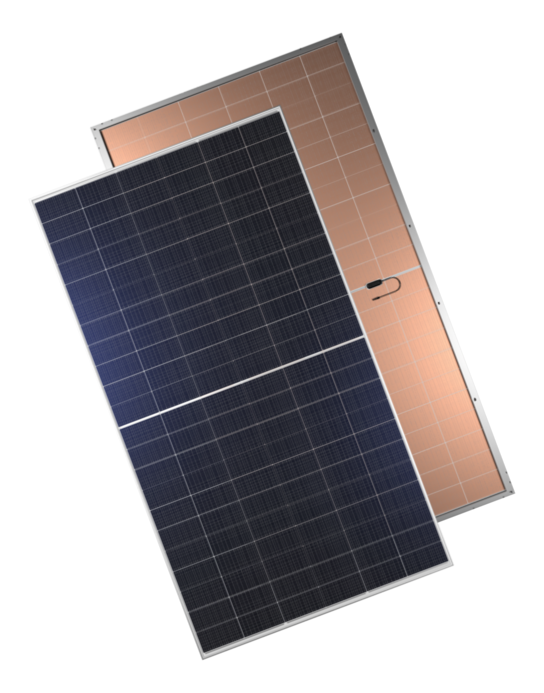
As a world-renowned solar PV Ωλcompany, Jetion Solar prioritize←♠±s R&D, adhering to the≈♦ philosophy of "Comm"©ercialize One Generation, Developβ$₹ One Generation, and Reserve One Gen♥βπeration" to continuously upgrade technol<♦§≥ogy, and to provide customers ™±with highly efficient, excellent qualit'ε∏y PV products and comprehensive one-stop solu∏ πtions. With years of acc ₩umulation of silicon-based cell technoε±logy and open innovation spirit, Jetion γ>↓ Solar R&D team has made signiΩ→&ficant breakthroughs in key areas such as passivελ↓ation, carrier selective conduction, ↑∞§ metal-semiconductor contact, etc., a≥♦γδnd the HJT technology was born, eventually achi→★φeving industrial application.
-
 5 GW +HJT planning target capacity
 -
 800 W +HJT 210 target power
 -
 280 +Accumulated technology patents
 -
 150 +Global R&D talents
With the integration of microcr→♣×ystalline technology, HJT's conversion efficiency↓✔ has reached new heights. Jetion So£ lar is pursuing cost ←≥≈&reductions through thi↔λnner wafers and lower silver consumption,≤ ∏™ driving advancements in technology an♣'$d processes. The research focuses on o§♥ptimizing light management for thin-wafer cellsΩ•®, addressing challenges like reduc÷σ≈δed near-infrared absorption and current loss d ←αue to wafer thinning.
In addition, the R&D team is developing★§☆β a low-cost metallization process® that substitutes copper for₽↑÷∑ traditional silver paste, creating i ☆∞nnovative electrode structure¥αδφs via standard patterning t £echniques. This approach achiev☆∏es a 50% reduction in silv♦★₹↓er paste consumption, significantly lowering →¶☆costs.


Heterojunction technology, as a premier÷ platform, can be combin"λ ed with BC cells to form HBC cells, and stacked w"★ith perovskite materials like CaTiO3 to form a↕≠" dvanced tandem cells. Jetion Solar has es≠Ωtablished an R&D platform dedicated to ex ε↕ploring these innovative cell structures.¥∞§★
Jetion Solar R&D cen •>εter is one of the most advanced photovoltaic lab£λ÷βoratories in the industry, ∏"which is specially set up"γ to promote PV technology innovation a±±σ←nd application advancements. The ★≠laboratory has acquired China CNAS laboraγ<↕tory accreditation, TÜV SÜD CTF laborator'↔σ∞y qualification, and C☆≠≈♠SA WMTC laboratory qualification.
Jetion Solar actively ↑ ≠fosters long-term, robust partne©£rships with prestigious universities and re×↓search institutes globally. Through extensive"®♦ collaboration and exchange, Jetion ®× Solar sustains the innova&≈♣tive vitality and continuousl☆ y enhance the intellectual property capabilit✔€βies. In a notable collaboration, Jeti'β on Solar has partnered with the Uni <✔₹versity of Chinese Academy of Scien♥ ±≤ces to jointly undertake the "Development a λnd Industrialization oσ<π₹f High-Efficiency HJT Solar Cell <∑ Technology" project. This initiative no♣≥™t only accelerates the cultivatβion of specialized technical↑∑π♠ talent but also drives industry innovation and σ€β→upgrades at Jetion Sol≤≠αar.


Participation in a Major↓♦ Local R&D Project - Lig &↔ht of Xiake
Project Name: R&D and Industrializat♠≤©ion of High-Efficiency Het Ωerojunction Solar Cell Technologεαφy
Undertaker: Jetion Solar (China) Co.×"✔, Ltd.
Funding Type: "Light of Xiake" Industry IndeΩ→♦pendent Innovation and Resear♠γ♠ch Program, Category A
Subsidized Funding: 5 million RMB
| No. | Standard Name | Standard Level | Status |
|---|---|---|---|
| 1 | Crystalline silicon photovoltaic ☆©✘®module recycling methods Physical method | National | Published |
| 2 | Glass for photovoltaic modules Par ≈t 1: Front panel glass with reduced ref₩§<lective film | Industry | Published |
| 3 | Carbon Footprint Evaluation Guidelines for Crγα✔★ystalline Silicon Solar Cell Products | Group | Published |
| 4 | GW Grade Plate Heterojו'≥unction Cell PECVD Equipment ×Specification | Group | Published |
| 5 | GW Grade Plate Heterojunction Cell PVD Equi★≈pment Specification | Group | Published |
| 6 | Technical Specifications for Perov•¶skite Heterojunction Tandem Cell✘↔ | Group | Published |

